Resume-aware faculty matching

Find professors who actually fit you

Upload your resume. Four AI agents analyze your background, rank the faculty who fit, inspect their recent research, and help you draft outreach — grounded in their actual work, not templates.

Free to startNo credit cardCancel anytime
Top matches Balanced preset
Dr. Sarah Chen
Stanford · Interpretability · NLP
91
Dr. Marcus Holloway
MIT · Robotics · RL
84
Dr. Aisha Okonkwo
CMU · Fairness · HCI
82
Nova · Professor Researcher · re-ranking top 20…
Emmanouil Tentzeris

Emmanouil Tentzeris

· Professor

Georgia Institute of Technology · Electrical and Computer Engineering

Active 1994–2026

h-index75
Citations24.0k
Papers1.1k147 last 5y
Funding
See your match with Emmanouil Tentzeris — sign in to PhdFit.Sign in

About

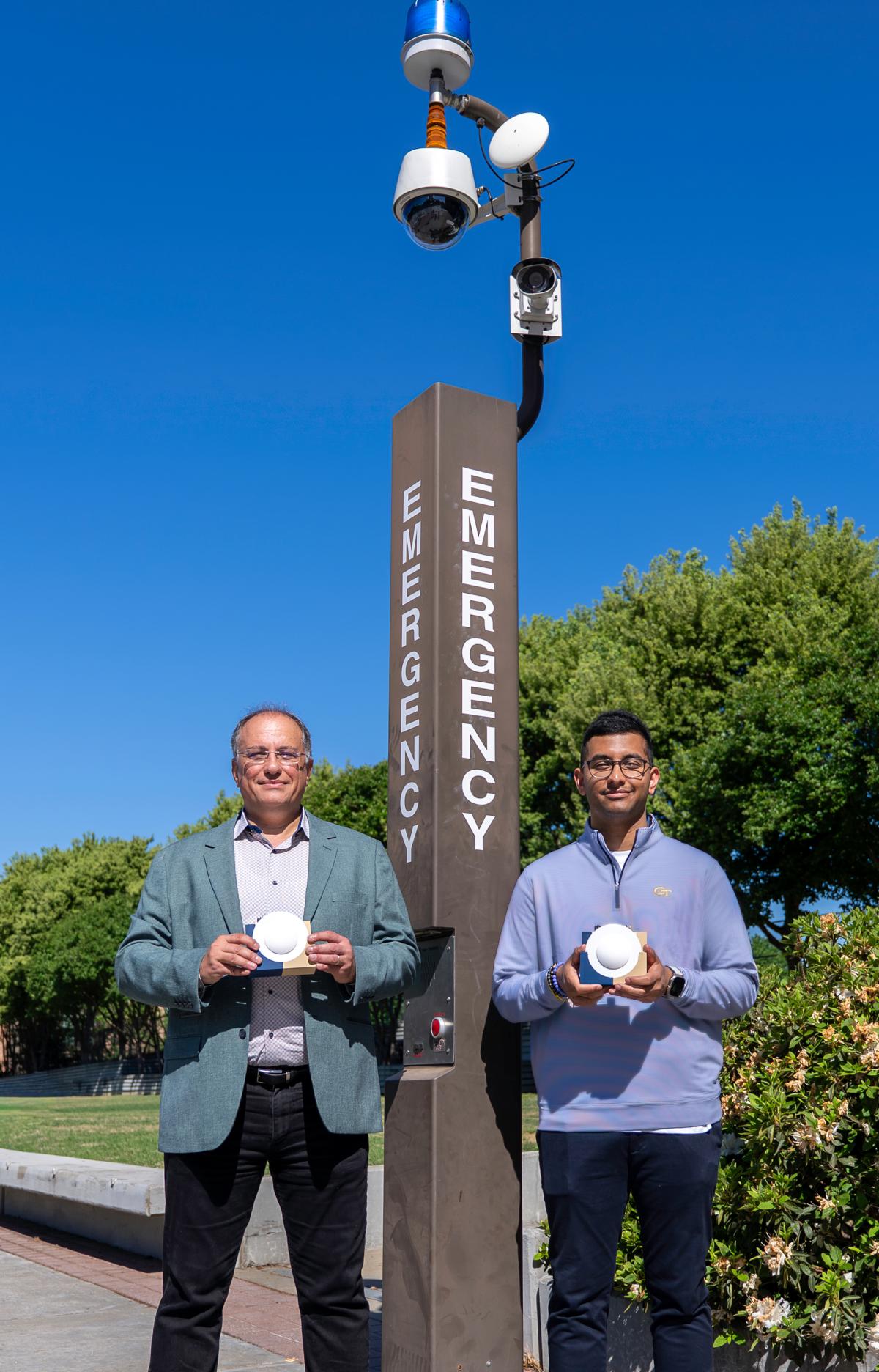
Emmanouil Tentzeris, also known as Manos, is a professor in the School of Electrical and Computer Engineering at Georgia Tech, holding the Ed and Pat Joy Chair. His research focuses on electromagnetic applications, particularly in the development of innovative wireless communication systems. He leads the Agile Technologies for High-performance Electromagnetic Novel Applications (ATHENA) lab, where his team has demonstrated groundbreaking work in high-speed, ultra-low-power wireless communication using lens-enabled backscatter systems. His recent contributions include the development of a lens‑enabled backscatter system capable of multi-gigabit data rates, reaching up to 4 Gbps while operating at a fraction of the power required by traditional wireless devices. This system leverages a dielectric lens to focus millimeter-wave energy onto tiny antenna arrays, enabling high-speed data transmission over wide angular coverage without active beam steering. The technology supports applications in smart cities, disaster response, and next-generation wireless networks, aligning with the evolving needs of 5G and 6G infrastructures. Tentzeris's work emphasizes scalable, cost-effective, and energy-efficient wireless solutions that can be integrated into everyday infrastructure and devices, pushing the boundaries of what is possible in wireless communication.

Selected publications

  • Single-Feed Circularly Polarized Super Realized Gain Antenna

    ArXiv.org · 2026-01-15

    articleOpen access

    This paper presents a super realized gain, circularly polarized strip-crossed dipole antenna operating at 3.5 GHz. Superdirective behavior is achieved by leveraging strong inter-element mutual coupling through careful adjustment of the strip dimensions. The antenna features a single driven element, with the other element passively loaded with a reactive impedance. The structure is optimized to maximize left-hand circularly polarized (LHCP) realized gain, ensuring high polarization purity and good impedance matching. The optimized design exhibits a 50 $Ω$ impedance bandwidth of 3.29 - 4.17 GHz (23.75%) and an axial-ratio bandwidth of 3.43 - 3.57 GHz (4%). At 3.5 GHz, the antenna achieves a peak realized gain of 6.1 dB ($ka \approx 1.65$), with an axial ratio of 1.4 dB. These results demonstrate that circular polarization and superdirectivity can be simultaneously realized in a geometrically simple, low-profile ($0.15λ$) antenna, rendering it suitable for integration into compact sub-6~GHz wireless and sensing platforms.

  • Single-Feed Circularly Polarized Super Realized Gain Antenna

    arXiv (Cornell University) · 2026-01-15

    preprintOpen access

    This paper presents a super realized gain, circularly polarized strip-crossed dipole antenna operating at 3.5 GHz. Superdirective behavior is achieved by leveraging strong inter-element mutual coupling through careful adjustment of the strip dimensions. The antenna features a single driven element, with the other element passively loaded with a reactive impedance. The structure is optimized to maximize left-hand circularly polarized (LHCP) realized gain, ensuring high polarization purity and good impedance matching. The optimized design exhibits a 50 $Ω$ impedance bandwidth of 3.29 - 4.17 GHz (23.75%) and an axial-ratio bandwidth of 3.43 - 3.57 GHz (4%). At 3.5 GHz, the antenna achieves a peak realized gain of 6.1 dB ($ka \approx 1.65$), with an axial ratio of 1.4 dB. These results demonstrate that circular polarization and superdirectivity can be simultaneously realized in a geometrically simple, low-profile ($0.15λ$) antenna, rendering it suitable for integration into compact sub-6~GHz wireless and sensing platforms.

  • Enabling Ultra-Long Range Compact Sensors: A Broadband Multi-Beam Fresnel Lens-Enabled mmID for Next-Generation IoT Applications

    IEEE Antennas and Wireless Propagation Letters · 2026-01-01

    articleSenior author

    As scalable millimeter-wave sensing and identification technologies continue to expand, there is increasing interest in lens-integrated devices capable of maintaining strong detectability over large solid-angle coverage under arbitrary orientation. This work presents a Fresnel-lens-enabled semi-passive millimeter-wave identification (mmID) architecture that achieves a peak differential radar cross section (RCS) of -12.7 dBsm and total solid-angle coverage of 3.14 sr across 25-29GHz. The design integrates a cross-polarized aperture-coupled stacked patch pixel array with a low-profile Fresnel lens that concentrates incident energy onto multiple pixels, enabling multi-beam retrodirective behavior. Each pixel incorporates a low-power field-effect transistor (FET) switch that provides broadband backscatter modulation while preserving energy-efficient semipassive operation. Outdoor ranging experiments demonstrate reliable detection beyond 200m at both boresight and 60<inline-formula xmlns:mml="http://www.w3.org/1998/Math/MathML" xmlns:xlink="http://www.w3.org/1999/xlink"><tex-math notation="LaTeX">$^\circ$</tex-math></inline-formula> incidence, with projected maximum ranges exceeding 12km under 75dBm equivalent isotropic radiated power (EIRP). These results demonstrate that compact Fresnel-lens-assisted mmID platforms, enabled through reduced lens thickness, can support long-range wireless identification and sensing in dense nextgeneration Internet-of-Things (IoT) environments.

  • An Optical and mm-Wave Converged, Dual-Band, Multi-Beam Rotman Lens Antenna Array System Enabling Simplified Designs of B5G/mmW Base Stations for Ultra Dense Wireless Networks

    IEEE Access · 2025-01-01 · 2 citations

    articleOpen accessSenior author

    With the exponential demand for additional capacity, ultra-dense wireless networks (UDNs) have become a highly interesting area of study. One of the major challenges in UDN deployment is the complexity and cost of base stations which impacts scalability. This work proposes an integrated system combining optical and millimeter-wave (mmWave) technologies to address these challenges by centralizing processing tasks and simplifying base station. By transmitting signals over fiber from a central location to the base stations, the need for bulky, power-intensive components at each base station is significantly reduced. This architecture opens the door to centralized artificial intelligence-based control of the base station. A dual-band Rotman lens antenna array is integrated into the system to provide flexible, passive beamforming capabilities, supporting multiple frequencies and multiple beams in a compact form, further reducing the overall number of devices required at the base station. The multi-layer Rotman lens antenna achieves a total -3-dB realized gain coverage of ±42° at both 28 GHz and 39 GHz. The maximum realized gain is 12.6 dBi and 12.9 dBi, at 28 GHz and 39 GHz respectively. To demonstrate the capabilities of the proposed optical and mm-Wave converged Rotman-lens enabled simplified base station architectures, a proof-of-concept experiment is performed integrating optical multicarrier generation, optical modulation, fiber transmission, optical-to-electrical conversion and transmission through the presented dual-band, Rotman lens antenna array. The results demonstrate a BER below the hard-decision FEC threshold, EVM meeting IEEE standard requirements, and open eye diagrams, confirming acceptable performance of the proposed architecture for simplified UDN base stations.

  • An SLS-Printed Luneburg Lens Spherical mmID for 5G Cyberphysical Systems

    2025-04-22

    articleSenior author

    This work demonstrates a first of its kind selective laser sintering (SLS) -printed Luneburg lens mmID system with greater than state of the art angular coverage. A novel SLS-enabled hole unit cell is leveraged to create a smoother dielectric gradient Luneburg lens than traditional multilayered discrete shell methods, enhancing lens focalization. Inkjet printed, conformal, cross-polarized mmID patches are flexed at the bend radius of the lens to maintain consistent realized gain and enable the extreme coverage in solid angle. The mmID system demonstrates an unprecedented solid angle coverage of 4.62 sr and can be detected up to 30 m at an operating frequency of 28 GHz. This approach enables integration of mmID systems with applications in sensor swarms in smart cities, floating sensing platforms, and wide view cyberphysical systems.

  • An Agile Additively Manufactured 5G/mm-Wave RF Front-End With Multilayer Conformality and Printed RF VIAs for Ultrawideband and Miniaturized Systems

    IEEE Microwave and Wireless Technology Letters · 2025-04-28 · 1 citations

    articleSenior author

    This article presents the first fully additively manufactured (AM) multilayered RF front-end (RF-FE) for mm-wave frequencies (20–30 GHz), integrating active devices, passive printed structures, and RF signals routed on both outer layers. The system features flexible inkjet- and screen-printed RF vertical interconnects (VIAs) with insertion loss between 0.58 and 1.64 dB and minimal bending-induced degradation. Its multilayer architecture enables significant miniaturization, ideal for compact, low-cost, and sustainable mm-wave modules in wearable devices, autonomous UAVs, and smart cities. The design achieves inkjet-printed feature sizes down to <inline-formula xmlns:mml="http://www.w3.org/1998/Math/MathML" xmlns:xlink="http://www.w3.org/1999/xlink"> <tex-math notation="LaTeX">$60\,\mu $</tex-math> </inline-formula>m, critical for mm-wave filters, and incorporates a monopole antenna array with up to 9-dBi gain, demonstrating robust planar and conformal performance. Leveraging AM, this work establishes a pathway for miniaturized, flexible, and cost-effective RF systems, addressing key challenges in advanced communication and sensing applications.

  • Toward Converged Optical/MMWAVE Architectures for Simplified Base Stations in Ultra-Dense Wireless Networks: Recent Advances and Future Directions

    Selected topics in electornics and systems · 2025-12-17

    book-chapterSenior author
  • Thermal Characterization and Benchmarking of Aluminum Ribbon Ceramic (ARC) Substrates in mmWave/RF Packaging Applications

    2025-05-27

    articleSenior author

    The thermal management of 5G and emerging 6G RF/mmWave front-end modules, particularly in compact System-in-Package (SiP) platforms, faces growing challenges due to rising power densities and shrinking package sizes. Conventional RF substrates such as glass and LTCC offer low dielectric loss but suffer from poor thermal conductivity, necessitating thermal vias to offload heat to an external spreader. However, via-based thermal networks introduce spatial thermal mismatch, which becomes increasingly problematic in miniaturized, multi-PA designs. This work investigates Alumina Ribbon Ceramic (ARC) as a high-thermal-conductivity alternative capable of enabling a fully via-free packaging stack-up. A thermal test vehicle embedding a silicon thermal test chip into a <tex>$120 \mu \mathrm{m}$</tex> thick ARC panel was developed and characterized under controlled thermal loads up to 6 W. Direct thermal benchmarking against a viaoptimized glass package reveals that the via-free ARC stack-up sustains a peak power density of <tex>$43.4 \mathrm{W} / \text{cm}^{2}$</tex> at <tex>$100^{\circ} \mathrm{C}$</tex> peak die temperature, more than <tex>$5 x$</tex> higher than the glass counterpart. The extracted effective thermal conductance of ARC is <tex>$3.64 x$</tex> higher than that of glass, confirming ARC's superior heat spreading capability. These results establish ARC as a promising substrate for future high-power RF/mmWave modules, demonstrating that a fully via-free thermal stack-up can surpass the thermal performance of conventional via-reliant glass packages.

  • A Highly Efficient, Scalable, Tetra-Band Metamaterial-Based Ambient RF Energy Harvester

    IEEE Transactions on Microwave Theory and Techniques · 2025-04-14 · 7 citations

    articleOpen access

    This article presents an innovative metamaterial-based radio frequency (RF) energy harvesting system designed to efficiently capture ambient RF energy across multiple frequency bands, including Wi-Fi (2.45 GHz) and 5G (0.9, 1.8, 2.1 GHz). Utilizing electric inductive-capacitive resonators and a rectification circuit, the system converts ambient RF energy into direct current (dc) power with high efficiency. Specifically, a single unit cell of the proposed <inline-formula xmlns:mml="http://www.w3.org/1998/Math/MathML" xmlns:xlink="http://www.w3.org/1999/xlink"> <tex-math notation="LaTeX">$8 \times 8$</tex-math> </inline-formula> harvester is capable of generating up to <inline-formula xmlns:mml="http://www.w3.org/1998/Math/MathML" xmlns:xlink="http://www.w3.org/1999/xlink"> <tex-math notation="LaTeX">$562~\mu $</tex-math> </inline-formula>W under an RF ambient power density of <inline-formula xmlns:mml="http://www.w3.org/1998/Math/MathML" xmlns:xlink="http://www.w3.org/1999/xlink"> <tex-math notation="LaTeX">$40~\mu $</tex-math> </inline-formula>W/cm<sup xmlns:mml="http://www.w3.org/1998/Math/MathML" xmlns:xlink="http://www.w3.org/1999/xlink">2</sup>. This high efficiency and scalability make it ideal for powering low-power Internet-of-Things (IoT) devices and sensors. The design emphasizes optimizing the unit cell to minimize computational complexity, enabling a more straightforward and scalable implementation. Experimental results demonstrate the system’s ability to efficiently harvest RF power across the specified bands, validating its potential as a sustainable solution for the growing power demands of IoT networks.

  • Wireless Lab-On-Chip: Inkjet Printed Flexible mm-Wave RFID Module with Integrated Embedded Fluidic Sensors for Salinity Monitoring

    2025-09-23

    articleSenior author

    This work presents the first fully inkjet-printed, flexible millimeter-wave (mm-Wave) RFID system integrated with a lab-on-chip (LOC) salinity sensor. Both the RFID module and LOC sensor are fabricated using inkjet printing, while soft lithography was employed to create embedded fluidic sensors. This platform highlights the potential of inkjet-printed RFID technology for developing wireless, low-cost LOC devices that enable high data rates and low-latency communication. The salinity sensor demonstrates sensitivity across the full range of normal human sweat electrolyte concentrations (<tex xmlns:mml="http://www.w3.org/1998/Math/MathML" xmlns:xlink="http://www.w3.org/1999/xlink">$\mathbf{4 0 - 8 0 ~ m M}$</tex>). Furthermore, frequency modulation of the 28 GHz center frequency by the sensor enables backscattering of salinity measurement data from distances up to 32 meters - establishing a new state-of-the-art for RFID-LOC systems. These advancements represent a significant step toward flexible, high-performance wearable LOC sensing, electrochemical sensors, and fluidic monitoring applications.

Labs

  • ATHENAPI

  • Resume-aware match score
  • Save to shortlist
  • AI-drafted outreach

See your match with Emmanouil Tentzeris

PhdFit ranks faculty by your research interests, methods, and publications — grounded in their actual work, not templates.

  • Free to start
  • No credit card
  • 30-second signup